Today’s IoT sensors are all around us. We alluded to the increasingly widespread nature of this network of sensors in our article ‘4 Reasons You Should Be Talking About the Internet of Things’ a few years ago, and since then said network has only grown larger. At this point the IoT (and the innumerable sensors that comprise it) now affects countless industries, and impacts our lives in ways most of us don’t quite even recognize.
We have reached this point in large part thanks to a combination of technological innovation and proof of concept. That is to say, as the early years of the IoT proved the benefits of connected and intelligent systems, there was more incentive to expand those systems. And in expanding those systems, people across industries have come up with increasingly ingenious ways to connect technology for the good of the people and societies using it. Beyond ambitious and innovative thinking though, expansion has also been dependent on the IoT sensors themselves becoming more capable.
Forbes examined the quality of sensors in a 2019 article that rightly pointed out the growing need for robust and durable devices. As the article stated, “sensors must be resilient and strong in the face of harsh conditions.” It went on to explain that those harsh conditions include monitoring temperature, fluids, gases, vibration, sound, and even light. These ideas speak to some of the challenges we’ve already seen for IoT sensors; from devices managing home irrigation systems and exposed to the elements, to traffic sensors in “smart city” networks, the equipment has had to be engineered to withstand a variety of stress factors. And as the article noted, we have seen the development of powerful new materials (including nanomaterials) to address these challenges.
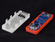
Those types of adjustments, however, speak primarily to the construction of IoT sensors on the outside, and where the actual “sensing materials” are concerned. Internal adjustments have also been required in some cases, simply because traditional electronics don’t always fit innovative sensor designs. This, indeed, is where PCBs (printed circuit boards) come into play.
The average PCB, while relatively small, is a rigid board built to house and connect electronic components within a device. The traditional flat, hard, chip-like structure, however, simply wouldn’t be compatible with a lot of modern IoT sensors. As a result, we’ve seen PCB designers explore more versatile options, such as “flex” PCBs. A look at flex PCB assembly by Altium reveals that these designs can allow for multiple PCBs to be linked together with improved adaptability and an ability to fit “odd” packages or smaller devices. They are in many cases, softer, bendable alternatives that are better able to contour as needed.
PCBs like this, as well as some other, increasingly compact designs, have helped to expand the possibilities for IoT sensors already — and will undoubtedly continue to do so in the coming years, as the demands continue to to become more complex. Techopedia’s piece on the IoT’s future noted recently in fact that we may soon need processor chips with “stronger memory capabilities and newer learning design” than the silicon chips commonly used today. New chips will present fresh challenges for the PCBs that house them and help to facilitate their performance, which means designers will have to continue to try new things.
Ultimately, a lot of different technology and engineering has gone into making the Internet of Things as massive and capable as it is today. As easy as it can be to forget about what actually makes the sensors tick though, it’s clear that PCBs and other internal components have played a major role in driving IoT sensors’ capabilities.